Latest Posts

RX和TX
Posted on: 2020-12-29 11:19:13 in Technology visited: 507在UART和ifconfig的命令中,都有RX,TX,这两个缩写是相同的,意思也是相同的。
对于ifconfig显示
RX==receive,接收,从开启到现在接收封包的情况,是下行流量。
TX==Transmit,发送,从开启到现在发送封包的情况,是上行流量。
对于UART
RX:接收数据pin
TX:发送数据pin

uboot i2c_set_bus_num注意事项
Posted on: 2020-12-26 18:22:32 in Technology visited: 828在uboot下使用i2c_set_bus_num使用完成后,最好对bus进行恢复,以防止其它部分访问时出错。
因为对i2c的访问函数,默认下对已经设置的i2c bus进行操作。
以下为从网上找到的代码片段,仅供参考
unsigned int orig_i2c_bus = i2c_get_bus_num();
i2c_set_bus_num(CONFIG_VIDEO_LCD_I2C_BUS);
i2c_reg_write(0x5c, 0x04, 0x42); /* Turn on the LCD */
i2c_set_bus_num(orig_i2c_bus);

uboot下的i2c命令解读与示例
Posted on: 2020-12-26 17:35:28 in Business visited: 5027
在uboot下输入i2c命令后,会返回以下信息。
其中的i2c dev/i2c probe/i2c speed较容易理解和使用。
但i2c md等命令说明不是常规的写法,解读起来有些困难。
uboot>i2c
i2c - I2C sub-system

Usage:
i2c crc32 chip address[.0, .1, .2] count - compute CRC32 checksum
i2c dev [dev] - show or set current I2C bus
i2c loop chip address[.0, .1, .2] [# of objects] - looping read of device
i2c md chip address[.0, .1, .2] [# of objects] - read from I2C device
i2c mm chip address[.0, .1, .2] - write to I2C device (auto-incrementing)
i2c mw chip address[.0, .1, .2] value [count] - write to I2C device (fill)
i2c nm chip address[.0, .1, .2] - write to I2C device (constant address)
i2c probe [address] - test for and show device(s) on the I2C bus
i2c read chip address[.0, .1, .2] length memaddress - read to memory
i2c write memaddress chip address[.0, .1, .2] length - write memory to i2c
i2c reset - re-init the I2C Controller
i2c speed [speed] - show or set I2C bus speed
在uboot的源代码cmd/i2c.c中有详细解释说明
i2c md chip address[.0, .1, .2] [# of objects] - read from I2C device
以执行命令i2c md 0x50 0.2 0x40为例子,从slave地址0x50(7位地址),从i2c设备的0x0开始(2个字节),读取0x40个字节
1: 0x50对应chip,是i2c的slave地址。
2: 0.2 对应address[.0, .1, .2],指两个字节的地址位,对应地址0x0000
3: 0x40为读取的数目,为16进制。
以执行命令i2c md 0x50 0x0f80.2 0x40为例子,从slave地址0x50(7位地址),从i2c设备的0x0f80开始(2个字节),读取0x40个字节
/*
* I2C Functions similar to the standard memory functions.
*
* There are several parameters in many of the commands that bear further
* explanations:
*
* {i2c_chip} is the I2C chip address (the first byte sent on the bus).
* Each I2C chip on the bus has a unique address. On the I2C data bus,
* the address is the upper seven bits and the LSB is the "read/write"
* bit. Note that the {i2c_chip} address specified on the command
* line is not shifted up: e.g. a typical EEPROM memory chip may have
* an I2C address of 0x50, but the data put on the bus will be 0xA0
* for write and 0xA1 for read. This "non shifted" address notation
* matches at least half of the data sheets :-/.
*
* {addr} is the address (or offset) within the chip. Small memory
* chips have 8 bit addresses. Large memory chips have 16 bit
* addresses. Other memory chips have 9, 10, or 11 bit addresses.
* Many non-memory chips have multiple registers and {addr} is used
* as the register index. Some non-memory chips have only one register
* and therefore don't need any {addr} parameter.
*
* The default {addr} parameter is one byte (.1) which works well for
* memories and registers with 8 bits of address space.
*
* You can specify the length of the {addr} field with the optional .0,
* .1, or .2 modifier (similar to the .b, .w, .l modifier). If you are
* manipulating a single register device which doesn't use an address
* field, use "0.0" for the address and the ".0" length field will
* suppress the address in the I2C data stream. This also works for
* successive reads using the I2C auto-incrementing memory pointer.
*
* If you are manipulating a large memory with 2-byte addresses, use
* the .2 address modifier, e.g. 210.2 addresses location 528 (decimal).
*
* Then there are the unfortunate memory chips that spill the most
* significant 1, 2, or 3 bits of address into the chip address byte.
* This effectively makes one chip (logically) look like 2, 4, or
* 8 chips. This is handled (awkwardly) by #defining
* CONFIG_SYS_I2C_EEPROM_ADDR_OVERFLOW and using the .1 modifier on the
* {addr} field (since .1 is the default, it doesn't actually have to
* be specified). Examples: given a memory chip at I2C chip address
* 0x50, the following would happen...
* i2c md 50 0 10 display 16 bytes starting at 0x000
* On the bus: A0 00 A1 ...
* i2c md 50 100 10 display 16 bytes starting at 0x100
* On the bus: A2 00 A3 ...
* i2c md 50 210 10 display 16 bytes starting at 0x210
* On the bus: A4 10 A5 ...
* This is awfully ugly. It would be nice if someone would think up
* a better way of handling this.
*
* Adapted from cmd_mem.c which is copyright Wolfgang Denk (wd@denx.de).
*/
参考执行示例
uboot>i2c dev
Current bus is 9
uboot>i2c dev 6
Setting bus to 6
uboot>i2c dev
Current bus is 6
uboot>i2c dev 9
Setting bus to 9

uboot>i2c md 0x50 0.2 0x40
0000: ff ff ff ff ff ff ff ff ff ff ff ff ff ff ff ff    ................
0010: ff ff ff ff ff ff ff ff ff ff ff ff ff ff ff ff    ................
0020: ff ff ff ff ff ff ff ff ff ff ff ff ff ff ff ff    ................
0030: ff ff ff ff ff ff ff ff ff ff ff ff ff ff ff ff    ................
uboot>
uboot>i2c probe 0x50
Valid chip addresses: 50
uboot>i2c probe 0xa0
Valid chip addresses:
uboot>i2c speed
Current bus speed=100000

uboot下的mii命令简介
Posted on: 2020-12-24 08:45:05 in Business visited: 6182uboot下有一个mii命令。命令帮助信息如下:
mii - MII utility commands

Usage:
mii device                     - list available devices
mii device            - set current device
mii info                 - display MII PHY info
mii read            - read  MII PHY  register
mii write     - write MII PHY  register
mii dump            - pretty-print   (0-5 only)
Addr and/or reg may be ranges, e.g. 2-7.
mii device示例,会输出MDC/MDIO总线设备
uboot>mii device
MII devices: 'FSL_MDIO0' 'FM_TGEC_MDIO'
Current device: 'FSL_MDIO0'
mii info打印输出,PHY后面跟的就是addr
uboot> mii info
PHY 0x00: OUI = 0x5043, Model = 0x1D, Rev = 0x01, 1000baseT, FDX
PHY 0x01: OUI = 0x0000, Model = 0x00, Rev = 0x00,  10baseT, HDX
PHY 0x02: OUI = 0x0000, Model = 0x00, Rev = 0x00,  10baseT, HDX
PHY 0x03: OUI = 0x0000, Model = 0x00, Rev = 0x00,  10baseT, HDX
PHY 0x04: OUI = 0x0000, Model = 0x00, Rev = 0x00,  10baseT, HDX
PHY 0x05: OUI = 0x0000, Model = 0x00, Rev = 0x00,  10baseT, HDX
PHY 0x06: OUI = 0x0000, Model = 0x00, Rev = 0x00,  10baseT, HDX
PHY 0x07: OUI = 0x0000, Model = 0x00, Rev = 0x00,  10baseT, HDX
mii read - read MII PHY register
mii write - write MII PHY register
上述两个命令,需要根据具体的芯片手册寄存器设置来进行配置。以下命令为示例
mii write 0 0 0x8000 向地址为0的phy芯片的0寄存器写入0x8000
mii read 0 0 读取地址为0的phy芯片的寄存器0的值

RJ45网口两个LED灯的指示意义以及控制原理
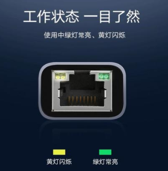
Posted on: 2020-12-23 21:50:51 in Business visited: 16008一般RJ45网口会有两个LED灯,至少从外观上看是两个。一个是link灯,一个是ACT灯。
参考下图所示,缺口朝上,一般右边绿灯常亮,表示link上,左边黄色、橘色、或者绿色灯闪烁,表示有数据传输。
有些act灯实际可能有多个是个多色灯,比如黄色、绿色。当100M时闪绿灯,当千兆时闪黄灯,以做区分。
这些灯是有PHY进行控制的。PHY的硬件接口文档中会有说明,以及相关的寄存器设置。
在uboot中可以使用mii来修改寄存器,改变亮灯状态。
在linux系统下,可以使用内核、驱动或者mii-tools修改控制灯的状态。
这些如何操作需要参考具体的硬件手册,因硬件手册厂家一般是不公开的,但从网上也能够找到零星的资料。
以下能够查找到的网上公开资料,可供参考

查centos的发行版本名称和版本号
Posted on: 2020-12-23 11:14:00 in Technology visited: 485rhel系统 cat /etc/os-release cat /etc/system-release cat /etc/redhat-release
centos系统 cat /etc/centos-release
fedora系统 cat /etc/fedora-release

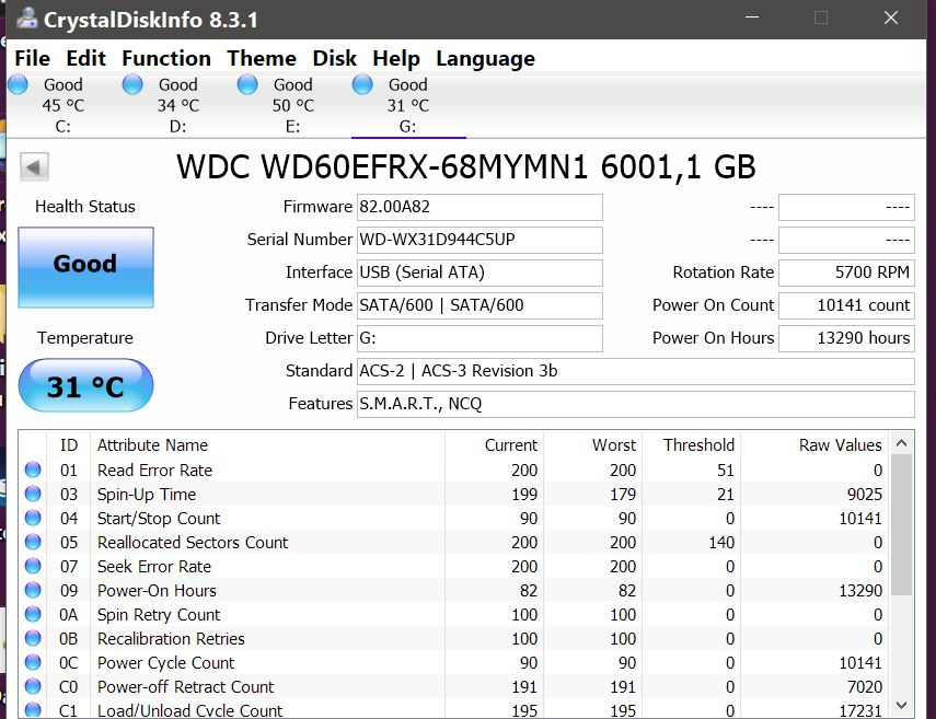
主轴起旋时间spin up time解释
Posted on: 2020-12-20 20:10:08 in Business visited: 812主轴起旋时间spin up time解释。
该词的来源是SMART Attribute。
| 03 | 03 | Spin-Up Time | Lower | Average time of spindle spin up (from zero RPM to fully operational). |
03(003)主轴起旋时间 Spin Up Time
主轴起旋时间就是主轴电机从启动至达到额定转速所用的时间,数据值直接显示时间,单位为毫秒或者秒,因此数据值越小越好。不过对于正常硬盘来说,这一项仅仅是一个参考值,硬盘每次的启动时间都不相同,某次启动的稍慢些也不表示就有问题。
硬盘的主轴电机从启动至达到额定转速大致需要4秒~15秒左右,过长的启动时间说明电机驱动电路或者轴承机构有问题。旦这一参数的数据值在某些型号的硬盘上总是为0,这就要看当前值和最差值来判断了。
对于固态硬盘来说,所有的数据都是保存在半导体集成电路中,没有主轴电机,所以这项没有意义,数据固定为0,当前值固定为100。
Spin-up time - is the time required to accelerate the disk to operating speed. Frequently used drives are often left spinning to improve access time, but drives may be spun down to reduce energy use or noise.


CentOS7图形界面与命令行界面切换
Posted on: 2020-12-19 16:23:27 in Business visited: 411| 方法一 |
开机以命令模式启动,执行: systemctl set-default multi-user.target
开机以图形界面启动,执行: systemctl set-default graphical.target |
| 方法2 |
命令行界面下进入图形界面 startx |
| 方法3 |
图形界面下显示命令行 ctrl+alt+F2 在这个命令行界面再返回图形界面 alt+F1或者 ctrl+alt+F1 |
| 方法4 |
在命令上 输入 init 3 命令 切换到dos界面 输入 init 5命令 切换到图形界面 |
